This week AMD has presented a rather detailed set of slides about their upcoming Zen micro-architecture to the press. Given their previous architectures (the Bulldozer family) I have to say I'm really impressed about the path they are now following (a step in the right direction for sure).
Processor block diagram and structures
Let's discuss the architecture at a high level: Zen is totally different to current AMD designs, and if you have been following the processor industry these years you will immediatly notice that Zen is very similar to Intel Core designs.
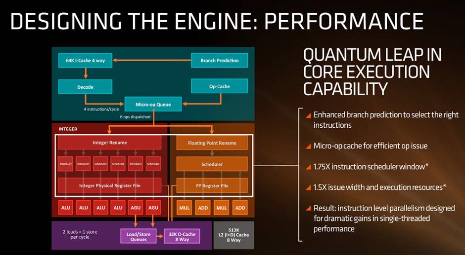
The core configuration is much more beefier than the one found in the Bulldozer family. Each core houses 1.5X the execution resources and 1.75X larger scheduler windows, which result in an enhanced abilty to extract instruction-level parallelism. This, at the end of the day translates into a rather large jump in IPC performance.
Intel has been constantly increasing the size of this strcutures in their designs, starting from their original 1st gen Core Architecture as a base. Given the similar design AMD is implementing with Zen we can expect competitive performance.
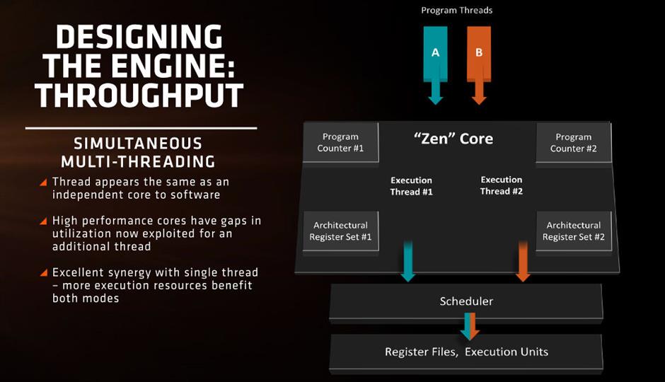
With the high increase in execution resources, the probability of having idle units at a given time also increases (no matter how large our scheduling windows may be, some instruction patterns might be impossible to execute in parallel). For this reason Zen also implements SMT capability like Intel processoros. This allows two threads to run over a single core, sharing all the execution pipeline with its resources, reducing possible pipeline stalls, and thus maximizing the core utilization.
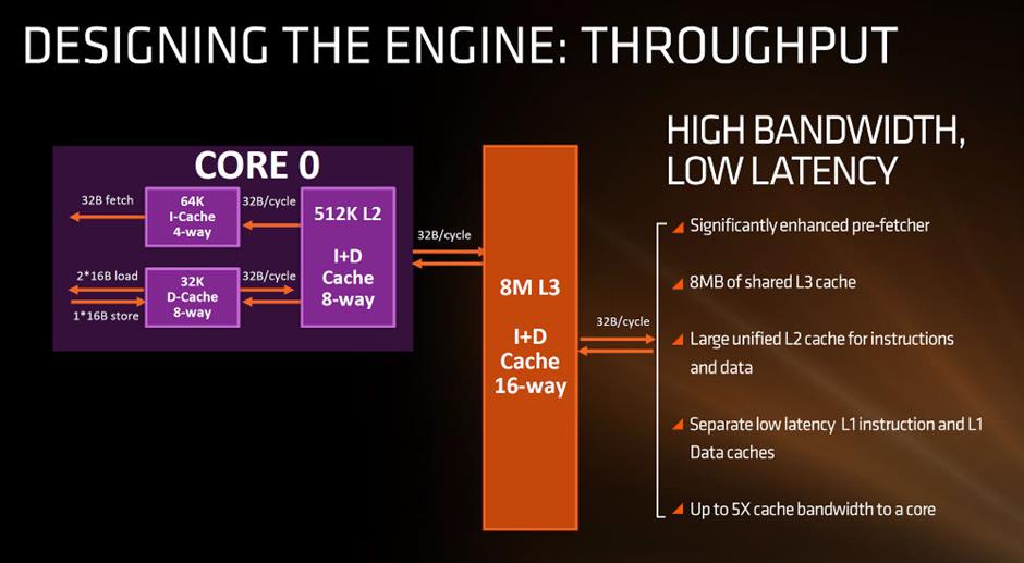
Not only the arrangement of structures is similar, but the cache hierarchy also follows the Intel route: the size, associativity and latency of the caches now are in line with Intel Core designs, even the cache policy used now changes back from Write-Through to Write-Back.
| | Bulldozer
FX-8150 | Zen | Broadwell-E
i7-6950X | Skylake
i7-6700K |
|---|
| L1I |
64 KB 2-way
per module |
64 KB 4-way |
32 KB 8-way |
32 KB 8-way |
| L1D |
16 KB 4-way
Write Through |
32 KB 8-way
Write Back |
32 KB 8-way
Write-Back |
32 KB 8-way
Write-Back |
| L2 |
2 MB 16-way
per module |
512 KB 8-way |
256 KB 8-way |
256 KB 4-way |
| L3 |
1 MB/core
64-way |
1 or 2 MB/core ?
16-way |
2.5 MB/core
16/20-way |
2 MB/core
16-way |
Power consumption and efficiency
Going a high-IPC route, has a noticeably impact in the final processor efficiency. As the processor does not need high frequencies to achieve a certain performance level, the overall power consumption is lower.
However the ability of high-clocking is always welcome, specially for gaming and single threading tasks.
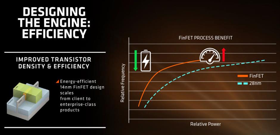
For this reason, Zen processors will be manufactured in a 14nm FinFET process (probably at GloFo or Samsung), which allows the design to clock even better than their predecesors and at the same point consume less power.
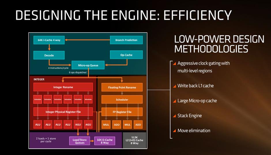
AMD explains the design is also heavily focused in efficiency through the implementation of clock gating, the write back cache policy, a micro-op cache and other tweaks.
Final thoughts
We believe AMD is in the right direction with their new Zen architecture. The core design is now wider and more complex aiming at high IPC, and higher thorughput just like Intel designs. If everything plays nice, we might finally get a decent competitor for the Intel Core series, and AMD will have a base microarchitecture to build over, for their next designs.